


产品与服务
- SFP+/QSFP+
- 6G SFP+
- 8G SFP+
- 10G SFP+
- 10G 单纤双向 SFP+
- 10G XFP
- 10G X2
- 10G XENPAK
- 10G 单纤双向 XFP
- 25G SFP28
- 40G QSFP+
- 100G QSFP28
- SFP
- 单纤 SFP
- 双纤 SFP
- 电口模块
- 1x9
- 1x9 非对称
- 1x9 单纤
- 1x9 双纤
- 单发单收
- CWDM光模块
- DWDM光模块
- PON光模块
- GPON ONU光模块
- EPON ONU光模块
- CABLE线缆
- 10G SFP+电缆
- 10G SFP+ Active 有源光缆
- 40G QSFP+ 电缆
- 40G QSFP+ Active 光缆
- Optical Sub Assembly
- BOSA
- EOC
- EOC终端
- 光无源器件
- CWDM波分复用器
- DWDM波分复用器
- AWG阵列波导光栅
- PLC分路器
- 光环形器
型号搜索 Model
特征搜索 Feature
 当前位置:首页 > 产品与服务 > SFP+/QSFP+ > 25G SFP28
 25G SFP28
HSFP8528-SRC
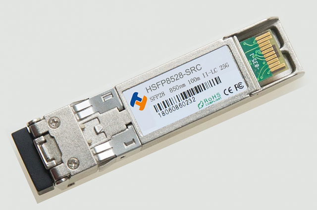
- 产品名称:HSFP8528-SRC
- 所属分类:25G SFP28
- 浏览次数:2318
- 上传时间:2018-08-28 14:02:34
|
|
|||||||||||||||||||||||||||||||||||||||||||||||||||||||||||||||||||||||||||||||||||||||||||||||||||||||||||||||||||||||||||||||||||||||||||||||||||||||||||||||||||||||||||||||||||||||||||||||||||||||||||||||||||||||||||||||||||||||||||||||||||||||||||||||||||||||||||||||||||||||||||||||||||||||||||||||||||||||||||||||||||||||||||||||||||||||||||||||||||||||||||||||||||||||||
|
|
|||||||||||||||||||||||||||||||||||||||||||||||||||||||||||||||||||||||||||||||||||||||||||||||||||||||||||||||||||||||||||||||||||||||||||||||||||||||||||||||||||||||||||||||||||||||||||||||||||||||||||||||||||||||||||||||||||||||||||||||||||||||||||||||||||||||||||||||||||||||||||||||||||||||||||||||||||||||||||||||||||||||||||||||||||||||||||||||||||||||||||||||||||||||||
Absolute Maximum Ratings
Electrical Characteristics(TOP=0 to 70 °C, VCC=3.135 to 3.465 Volts)
Note: 1. Connected directly to TX data input pins. AC coupling from pins into laser driver IC. 2. Per SFF-8431 Rev 3.0 3. Into 100 ohms differential termination. 4. 20%~80% 5. LOS is an open collector output. Should be pulled up with 4.7k – 10kΩ on the host board. Normal operation is logic 0; loss of signal is logic 1. Maximum pull-up voltage is 5.5V. Optical Characteristics(TOP = 0 to 70°C, VCC = 3.135 to 3.465 Volts)
Note: 1. Average power figures are informative only, per IEEE802.3ae. 2. TWDP figure requires the host board to be SFF-8431 compliant. TWDP is calculated using the Matlab code provided in clause 68.6.6.2 of IEEE802.3ae. 3. 12dB reflection. 4. Conditions of stressed receiver tests per IEEE802.3ae. CSRS testing requires the host board to be SFF-8431 compliant. 5. Receiver overload specified in OMA and under the worst comprehensive stressed condition.
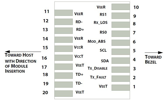
Pin Assignment
Pin Function Definitions
Note: 1. The module ground pins shall be isolated from the module case. 2. This pin is an open collector/drain output pin and shall be pulled up with 4.7K-10K ohms to Host_Vcc on the host board. 3. This pin shall be pulled up with 4.7K-10K ohms to VccT in the module. 4. This pin is an open collector/drain output pin and shall be pulled up with 4.7K-10K ohms to Host_Vcc on the host board.
|
|||||||||||||||||||||||||||||||||||||||||||||||||||||||||||||||||||||||||||||||||||||||||||||||||||||||||||||||||||||||||||||||||||||||||||||||||||||||||||||||||||||||||||||||||||||||||||||||||||||||||||||||||||||||||||||||||||||||||||||||||||||||||||||||||||||||||||||||||||||||||||||||||||||||||||||||||||||||||||||||||||||||||||||||||||||||||||||||||||||||||||||||||||||||||
|
公司荣誉
|
|||||||||||||||||||||||||||||||||||||||||||||||||||||||||||||||||||||||||||||||||||||||||||||||||||||||||||||||||||||||||||||||||||||||||||||||||||||||||||||||||||||||||||||||||||||||||||||||||||||||||||||||||||||||||||||||||||||||||||||||||||||||||||||||||||||||||||||||||||||||||||||||||||||||||||||||||||||||||||||||||||||||||||||||||||||||||||||||||||||||||||||||||||||||||
|
|||||||||||||||||||||||||||||||||||||||||||||||||||||||||||||||||||||||||||||||||||||||||||||||||||||||||||||||||||||||||||||||||||||||||||||||||||||||||||||||||||||||||||||||||||||||||||||||||||||||||||||||||||||||||||||||||||||||||||||||||||||||||||||||||||||||||||||||||||||||||||||||||||||||||||||||||||||||||||||||||||||||||||||||||||||||||||||||||||||||||||||||||||||||||
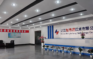
工厂实拍
|
|||||||||||||||||||||||||||||||||||||||||||||||||||||||||||||||||||||||||||||||||||||||||||||||||||||||||||||||||||||||||||||||||||||||||||||||||||||||||||||||||||||||||||||||||||||||||||||||||||||||||||||||||||||||||||||||||||||||||||||||||||||||||||||||||||||||||||||||||||||||||||||||||||||||||||||||||||||||||||||||||||||||||||||||||||||||||||||||||||||||||||||||||||||||||
关于我们 |
|||||||||||||||||||||||||||||||||||||||||||||||||||||||||||||||||||||||||||||||||||||||||||||||||||||||||||||||||||||||||||||||||||||||||||||||||||||||||||||||||||||||||||||||||||||||||||||||||||||||||||||||||||||||||||||||||||||||||||||||||||||||||||||||||||||||||||||||||||||||||||||||||||||||||||||||||||||||||||||||||||||||||||||||||||||||||||||||||||||||||||||||||||||||||
|
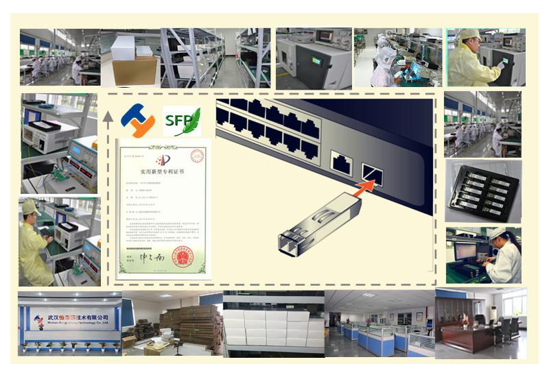
武汉恒泰通技术有限公司位于国家光通信发源地—“武汉·中国光谷”,是由国内一批资深光电子通信领域专家共同组建的专业从事通信用光电产品的研发、生产、销售、服务的高科技企业。 公司以市场为导向,研发为核心,长期坚持研发投入,并与各大通信公司、院校和科研单位保持良好的合作关系,致力于科技创新,保持行业的领先地位。拥有近2000平米的无尘净化车间,具备完整的生产线和生产设备,整套的测试与老化设备,完善的实验设备,执行严格的生产工艺和检验流程,具有卓越的品质保证。公司已通过ISO9001:2008质量体系认证,所有产品已通过ROHS,CE,FCC等相关认证。 公司主要生产有源光组件、有源光模块、光纤通信子系统三大系列产品,产品广泛应用于移动通信网络优化、通信网络、数据存储网络、高速FTTX、视频监控和交换机等领域。经过多年的运营和发展,公司已经建立起了一整套完善的供应链管理体系和成熟的配套供应资源,可以满足客户的低成本、高品质、交期快的要求。
追求卓越,实现梦想,恒泰通将秉承自主创新、质量为本的理念,不断完善管理,提高经营水平,为广大客户提供优质的产品和服务;锐意开拓,不断进取,恒泰通愿与广大合作伙伴携手共进,共创美好未来! |
|||||||||||||||||||||||||||||||||||||||||||||||||||||||||||||||||||||||||||||||||||||||||||||||||||||||||||||||||||||||||||||||||||||||||||||||||||||||||||||||||||||||||||||||||||||||||||||||||||||||||||||||||||||||||||||||||||||||||||||||||||||||||||||||||||||||||||||||||||||||||||||||||||||||||||||||||||||||||||||||||||||||||||||||||||||||||||||||||||||||||||||||||||||||||
 |
|||||||||||||||||||||||||||||||||||||||||||||||||||||||||||||||||||||||||||||||||||||||||||||||||||||||||||||||||||||||||||||||||||||||||||||||||||||||||||||||||||||||||||||||||||||||||||||||||||||||||||||||||||||||||||||||||||||||||||||||||||||||||||||||||||||||||||||||||||||||||||||||||||||||||||||||||||||||||||||||||||||||||||||||||||||||||||||||||||||||||||||||||||||||||